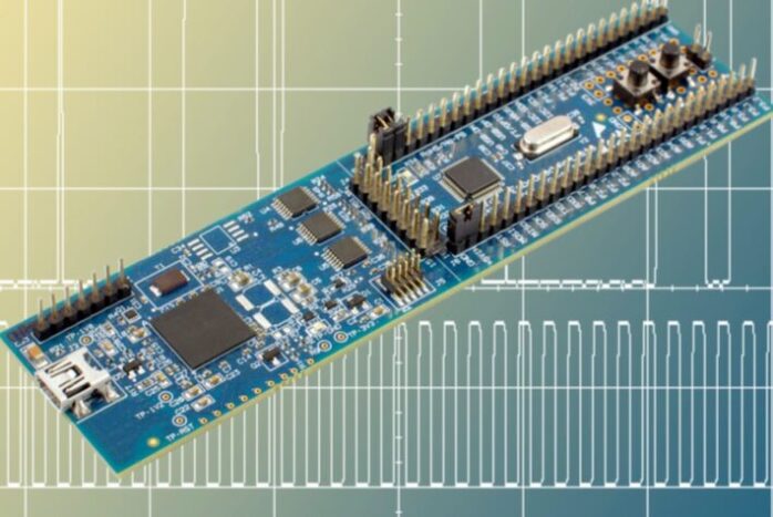
Do you want to design your PCB from scratch? And don’t know how to begin the process? Don’t worry, because we have created this article to help you with the same. We will share some essential tips for designing PCB from scratch. Designing PCB is indeed complicated for beginners, but with some guidance, anyone can do it.
One needs to take every step carefully while creating a design for PCB. However, if you are a beginner, you can get a PCB quote online as well. One should do proper research before getting into the procedure of planning the layout for it. As it is a long process, you need to be very focused from the beginning.
So, without wasting any time, let’s discuss some essential tips for the same.
7 Tips for making a design for a printed circuit board from scratch
1. Creating the electric schematic
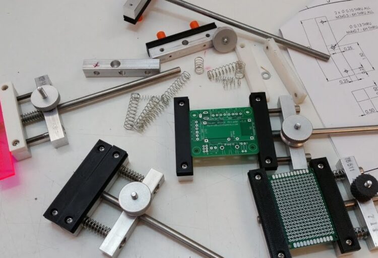
The first tip is to create the schematic. You can design it by using the software. One of the best software is Kicad, and you will find various options in it.
To make the schematic perfect, you must avoid errors while making the diagram for the same. Any small mistake will impact the layout of the printed circuit board. So, be careful and focused.
One solution to avoid making mistakes is to do the assembly process first. You can do it by using the diagram of the layout. You must name all the components correctly and also arrange the sections of the schematic in perfect order. Also, it is crucial to know the function of every block while doing this step.
2. Using the grid method
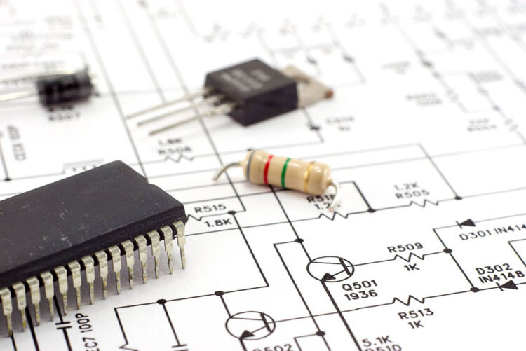
Grids are helpful while making a PCB design, especially if you are a beginner at this. The grid method is used in almost all projects because it helps people quickly draw out the elements accurately. So, while you are preparing a diagram, you can use a graph.
The development of the circuit is possible only when you arrange the components accordingly. One of the most significant things you should keep in mind is that all the elements should be symmetrical and aligned. And grids will help you achieve it.
Therefore, the grid method is an essential tool to arrange and order the components of the circuit in the diagram.
You can look for some examples on the web too. All you have to do is search for some printed circuit board design images and understand how it has been created using the grid method.
3. Calculating the tracks’ breadth
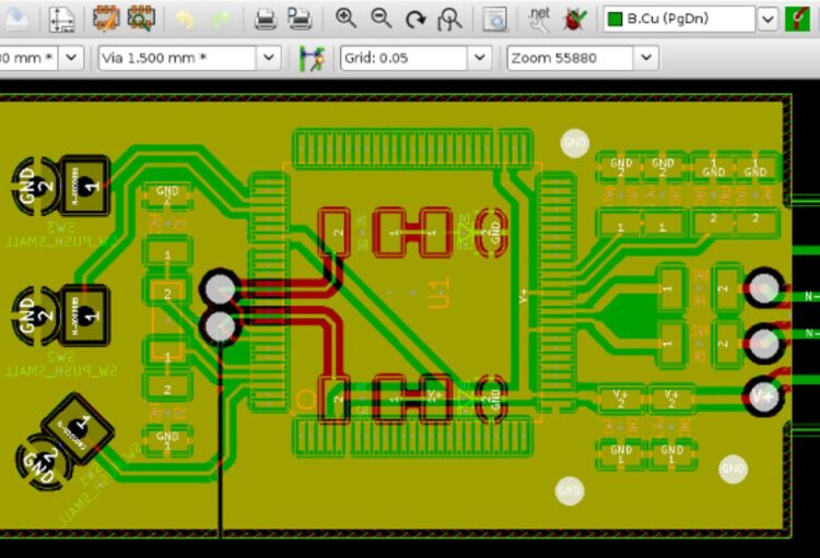
This is another essential tip you should consider while creating the layout—the tracks in the circuit act as wires to supply electricity through the entire system. But how can you calculate it?
You might already know that if the electric current value is higher, it needs a large conductor segment. Similarly, if the electric current value is lower, it needs a small conductor segment.
The system of the printed circuit board also works like this. There are various websites and applications available to calculate it, and you can use them to get an idea of the same.
One such website is Digikey, and here you can enter the value of electric current, thickness of the copper, temperature, and length of the track. After that, you will get two types of widths- for multilayer tracks and single and double layer tracks. Note down both of them to continue with the process of designing.
4. Understanding Auto Placement and Auto Router
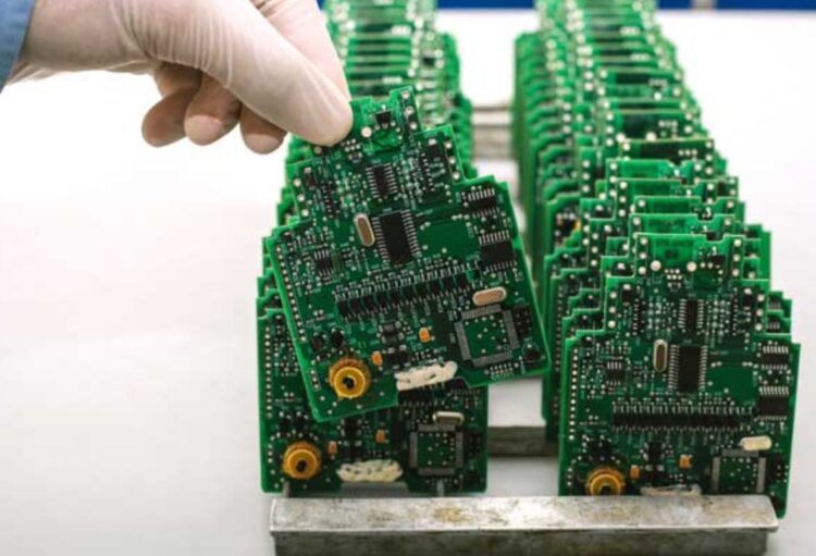
Auto-placement and auto-router are the two most used tools that every PCB designer should understand. Both of them are risky to use.
Auto-routing involves routing all the tracks by the software. Sometimes, this process disturbs the arrangement of the tracks. Many professionals and designers suggest not to use this tool unless you don’t know about it in detail.
The software that helps rout the tracks might not process the signal levels, various electronic elements, characteristics of the components, and more. As a result, it creates chaos in the system of the circuit.
Thus, you should avoid it at any cost. An alternative is manual routing; it will help you organize the elements correctly and ensure a better structure.
Similarly, auto-placement can cause issues in your project. It will automatically arrange the components without knowing their characteristics. You should also avoid auto-placement to create a perfect design for the printed circuit board. Always try to do these processes manually.

5. Using copper sections
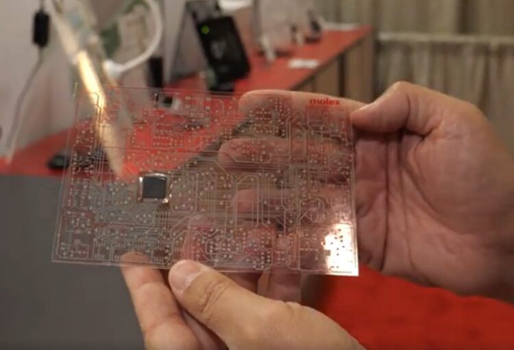
A common problem that happens in all the circuits is the loss of heat. The solution for this problem is using rectangular shape copper regions under the IC.
All the devices that are unable to work at high temperatures should be kept away from them. It is essential to place them in low-temperature regions of the PCB. This strategy will help you in improving the security of the circuit.
6. Silkscreen layer for printing information
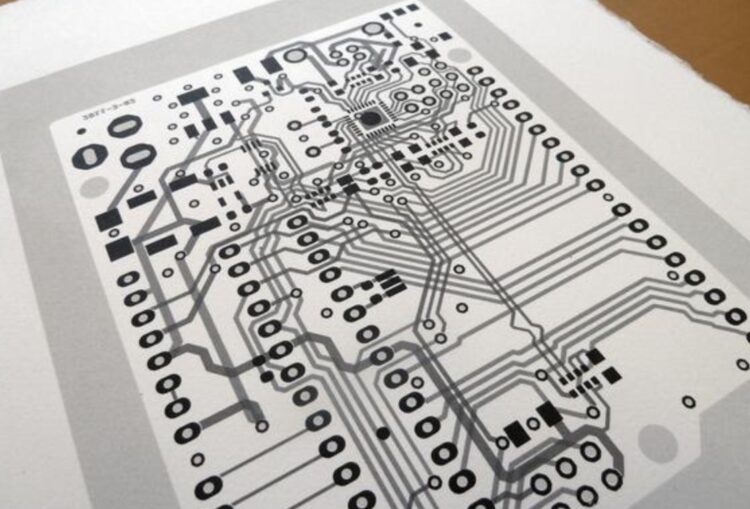
You should use the silkscreen layer for printing the information on the design. There are many advantages of using this layer. They are as follows-
- You can print the information about all elements and connections of the printed circuit board.
- If you want a maintenance process in the future, the user will quickly understand the information printed on the PCB.
- The design looks systematic with the help of this layer.
So, using the silkscreen layer will benefit you a lot as you can share the information with other users.
7. Creating the prototypes
It is possible to create the entire circuit at a low cost. To begin this, you first need to gain some knowledge about the same. Then, start creating the prototypes to build the layout for your first printed circuit board. You can also take help from different articles and videos to get started with it.
Final Words
In the end, we would like to say that making a design for the PCB is complicated but not impossible. We hope this article helped you in knowing some tips and tricks to create your first PCB layout. You can always refer to this article again if you need to learn about these tips in detail.


